High-NA EUV Needs a Bigger Window for Bigger AI Chips
Matthew Leo · Published September 13, 2026 · News
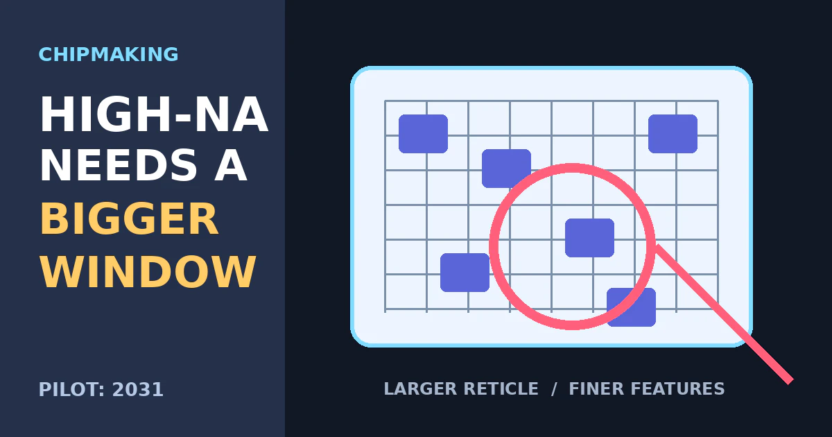
ASML's newest High-NA extreme-ultraviolet machines can draw finer chip features, but their current exposure field creates an awkward limit: the largest AI processors may be too big to print as one complete design.
ASML now plans to solve that problem with larger masks and matching changes across the lithography system. The company says it will work with major chipmakers on a pilot line in 2031 and target high-volume production in 2033.
That timeline makes this an important manufacturing roadmap, not a near-term promise that tomorrow's graphics cards will suddenly become cheaper or faster.
The problem is the printable field
A lithography machine projects patterns from a mask, also called a reticle, onto a silicon wafer. High-NA EUV uses a higher numerical aperture to print smaller features than conventional EUV, but its current field is narrower.
Existing EUV equipment can handle designs up to roughly 800 square millimetres. The narrower High-NA field can force a large processor to be divided across multiple exposures, a technique called stitching. That adds design and manufacturing complexity at the boundary between the sections.
A larger mask would let High-NA equipment preserve its finer resolution while accommodating chips closer to the size already used for large data-centre accelerators.
What ASML is proposing
According to Reuters' September 8 report, ASML plans new mask dimensions and system changes that would support larger designs. The company says the approach could improve system productivity by 40% compared with handling the same large design through the existing High-NA field.
That 40% figure is ASML's projection. It is not an independently measured production result from a mature 2033 factory.
The work also extends beyond ASML. Mask writers, inspection equipment, design software, process controls and chipmakers' factories all have to support the larger format. A better scanner cannot create an ecosystem by itself.
High-NA adoption is already staggered
- Intel is already using High-NA tools for some production work.
- Samsung and SK Hynix are targeting High-NA for DRAM production from 2028.
- TSMC has indicated adoption around 2030.
- ASML's larger-mask pilot is planned for 2031, followed by a 2033 high-volume target.
Each date is a company plan, not a guaranteed industry-wide switch. Chipmakers can continue improving conventional EUV through better optics, masks, process control and multiple patterning while they decide where High-NA makes economic sense.
Why AI processors make the limit visible
Large AI accelerators push close to the practical size limits of a single chip because more compute, cache and high-speed interfaces compete for area. Advanced packaging can combine several chiplets, but that does not eliminate the need to print large, defect-sensitive pieces efficiently.
The mask change is therefore less about making every transistor smaller than making finer lithography useful for the physically large processors driving data-centre demand. It connects two constraints that are often discussed separately: transistor density and total die area.
Mapletechie's analysis of Nvidia's infrastructure-heavy quarter showed how much capital is already chasing AI compute. Larger-mask High-NA equipment may eventually expand manufacturing options, but it also adds another costly transition for an industry already investing aggressively.
The practical takeaway
High-NA EUV is not being abandoned because its field is smaller. ASML and its customers are trying to widen the useful design space without giving up the resolution advantage.
The engineering idea is straightforward; the industrial execution is not. Watch the pilot results, ecosystem readiness, defect rates and cost per working chip. Those measures will matter more than the size of the mask alone.
Tags: ASML, High-NA EUV, semiconductors, AI chips